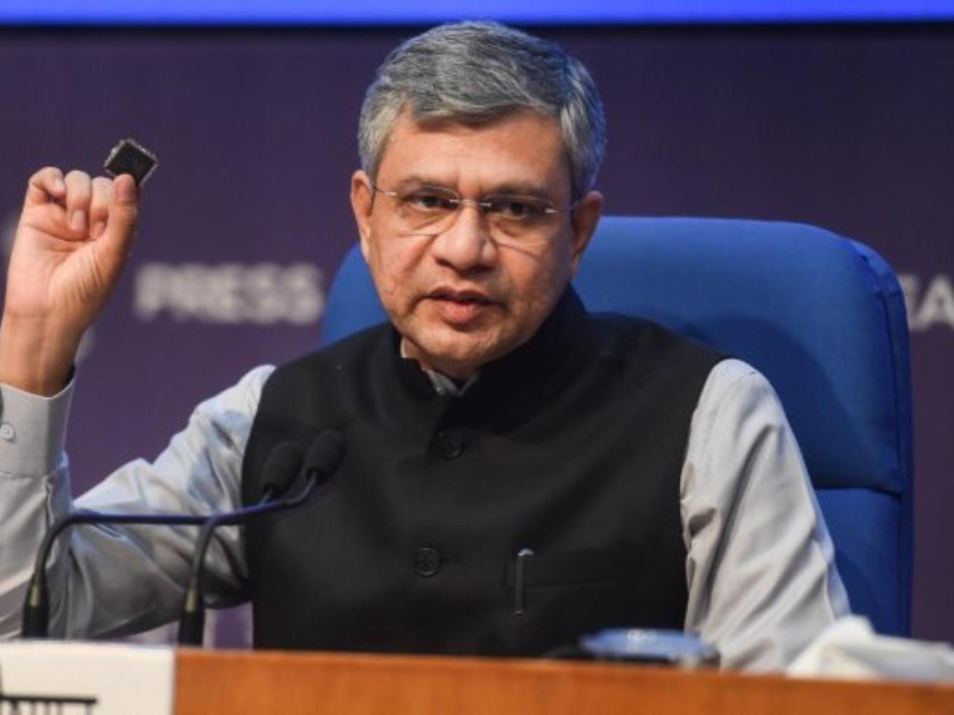
India is developing a commercial-scale silicon-based fabrication facility with an above average capacity of 50,000 wafer-starts per month, minister for electronics and information technology Ashwini Vaishnaw said.
“Six semiconductor units, one fab and five assembly, testing, marking and packaging units, are at different stages of planning, construction and execution. Four more (one silicon carbide fab and three ATMP including the most advanced packaging unit) were approved last week. The entire ecosystem – design, fabrication, packaging, equipment, chemicals, gases – taking shape in Bharat,” the minister said in an X post.
Major equipment manufacturers Applied Materials and Lam Research are setting up their design, production, and validation facilities in the country, he added.
In semiconductor manufacturing, a wafer is a thin, circular slice of a crystalline semiconductor material, most commonly silicon, integrated circuits are fabricated. Most silicon fabs usually operate at 20,000-40,000 wafer-starts per month.
Semiconductor Ecosystem Emerging As India’s Next Growth Driver
Ashwini Vaishnaw’s comments on India’s chipmaking roadmap comes just a few days after the Union Cabinet had approved four projects with a total investment of INR 4,584 Cr under the India Semiconductor Mission (ISM). Two of the projects will be in Odisha, and one each will be in Punjab and Andhra Pradesh.
Earlier in May, the ministerlaunched two new state-of-the-art design hubs in Noida and Bengaluru to bolster India’s semiconductor capabilities, from architecture to testing.
In 2022, the government of India launched the first phase of its semiconductor mission to establish the country as a global hub for electronics manufacturing and design.
This came a year after the government launched the Semicon India programme, infusing INR 76,000 Cr to incentivise silicon semiconductor fabs, display fabs, compound semiconductors, and more.
More than five semiconductor units have been approved under the ISM to boost India’s semiconductor landscape, expected to attract a total investment of INR 1.52 Lakh Cr.
Amitesh Kumar Sinha was named as the new chief executive officer of the India Semiconductor Mission in April this year, weeks after reports surfaced that the union government is internally discussing plans for the rollout of the second phase of the ISM, while also mulling “supporting” chip design projects in the country and semiconductor packaging designs.
At the heart of all this is the homegrown semiconductor market which, as per Inc42, is expected to become a $150 Bn opportunity by 2030.
The post India Setting Up Commercial Silicion Fab With 50,000 Per Month Wafer Capacity: Ashwini Vaishnaw appeared first on Inc42 Media.
Original Article
(Disclaimer – This post is auto-fetched from publicly available RSS feeds. Original source: Inc42. All rights belong to the respective publisher.)